

USB4 Cable Factory Essentials for 40Gbps Performance
2026-10-18
You've seen the spec sheet: 40Gbps, 8K video, 240W power. But have you ever wondered what actually happens on the factory floor to make those numbers real? At EBCYX, we obsess over the details most brands skip—because a USB4 cable is only as fast as its weakest solder joint. In this post, we're cracking open the essentials for manufacturing cables that truly deliver 40Gbps, not just promise it.
Conductor Purity Levels That Decide True 40Gbps Throughput
At high data rates like 40Gbps, the signal travels almost exclusively along the outer surface of a copper conductor—a phenomenon known as skin effect. Impurities trapped inside the metal don't just sit there; they scatter electrons and create localized resistance spikes that distort the rising edges of digital pulses. Even a fraction of a percent of oxygen or trace metals can turn a clean eye diagram into a smeared mess before the signal reaches the other end.
Not all copper is created equal. Standard electrolytic tough pitch (ETP) copper contains roughly 300–500 ppm of oxygen, which forms copper oxide islands at grain boundaries. These boundaries act as tiny reflectors, causing inter-symbol interference that becomes lethal at 40Gbps. Oxygen-free high-conductivity (OFHC) copper reduces oxygen to under 10 ppm, while single-crystal or Ohno continuous casting (OCC) copper goes further by eliminating most transverse grain boundaries entirely—giving electrons a nearly uninterrupted path.
For a cable to deliver true 40Gbps throughput without negotiation downshifts or packet retries, the conductor purity must be paired with precise drawing and annealing processes. Too many manufacturers stamp '40Gbps' on the jacket while using recycled copper with uncertain impurity profiles. The result is a link that trains at full speed during idle but collapses under sustained traffic or longer runs. Only by keeping oxygen below 5 ppm and controlling grain orientation can a conductor maintain the signal integrity margins required by modern high-speed interfaces.
Shielding Architecture That Holds Up Under Repeated Flexing
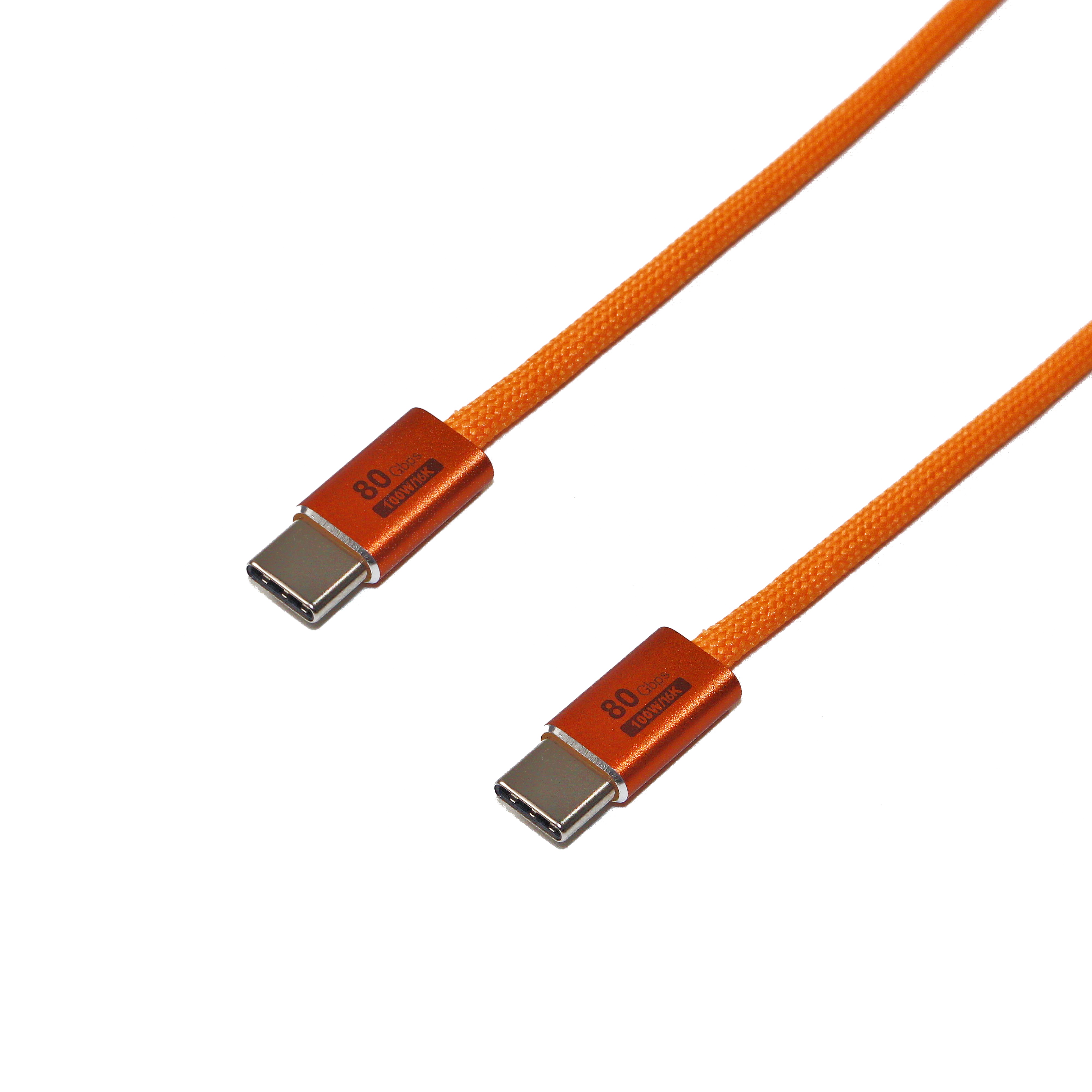
In flexible cable assemblies, the shield is often the first layer to crack under repeated motion. A braided construction spreads mechanical stress more evenly than a spiral wrap, but even fine-wire braids can snap individual strands at tight bend radii. The architecture most likely to survive dynamic flexing pairs a high-strand-count braid with a low-friction separator tape, letting the wires slide slightly instead of grinding against one another.
Another route skips the classic braid entirely. Laminated foil shields, sometimes backed with a conductive polymer, deliver better flex life in continuous bending applications. The trade-off shows up as lower coverage at higher frequencies unless the foil is bonded to a reinforcing film that resists cracking. Choosing a shield architecture for flexing environments means testing candidates under the actual bend profile and torsion conditions the assembly will face, not relying on static shielding effectiveness numbers.
Connector Termination Details That Keep Signal Eyes Open
A clean eye diagram starts long before the test fixture gets powered up. In high-speed interconnects, the way a shield drain wire is folded, the exact length of exposed center conductor, and the amount of solder wicked up a cup can each nudge impedance just enough to close the eye. Paying attention to these seemingly small termination details—like trimming braid without nicking the dielectric and keeping the untwisted region under 3 mm for differential pairs—means the difference between a link that runs at spec and one that fails intermittently when the chassis flexes.
Crimp terminations get a bad reputation when they are treated as purely mechanical joints. A reliable gas-tight crimp actually requires matching the wire barrel to the conductor's cross-sectional area and using a tool with the correct die profile. Too little compression leaves voids that oxidize over time, raising contact resistance and adding low-frequency jitter. Too much compression can fracture strands or distort the connector body enough to misalign the mating interface. The same applies to solder terminations: a concave fillet with no sharp spikes reduces stress risers, and pre-tinning stranded wire prevents stray filaments from touching an adjacent pin or the shell.
Grounding and shield termination often decide whether a channel stays open. Instead of letting a drain wire meander to a single solder point, many designs now use 360-degree shield termination through a conductive ferrule or a wrap-around pad that presents a low-inductance path at the connector entry. For board-mount connectors, placing ground vias close to the signal pins and keeping the pad shape symmetrical around each differential pair discourages common-to-differential mode conversion. These details are not glamorous, but they keep the eye from squinting when rise times shrink and link budgets tighten.
Production-Line Testing That Catches Marginal USB4 Cables
USB4 cables carry data at up to 20 Gbps per lane, so a marginal cable that passes basic continuity can still produce occasional bit errors under real signal conditions. Production-line testing must go beyond simple wire mapping and look at signal integrity margins: time-domain reflectometry to spot impedance discontinuities, insertion loss up to 10 GHz, and near-end crosstalk between lanes.
A practical approach uses a vector network analyzer or dedicated cable tester to compare measured S-parameters against a golden cable envelope. Instead of pass/fail at one frequency, the system sweeps multiple frequencies and flags any pair or shield connection that dips too close to the limit. This catches cables with slightly loose crimps or uneven dielectric that would only fail after thermal cycling or repeated bending.
To verify margin, some lines add a short bit-error-rate test with a known stressed pattern, then apply a small amount of attenuation or jitter. If the cable survives that added stress but still recovers data, it has enough headroom for end-user systems. This combined approach catches marginal USB4 cables before they leave the factory, reducing returns and intermittent field failures.
Keeping Differential Impedance Stable Across Every Batch
Batch-to-batch variation in differential impedance rarely comes from a single dramatic failure. It sneaks in through small, cumulative shifts: a laminate vendor changing resin formulation slightly, copper foil roughness drifting a few microns, or prepreg flow behavior reacting differently to a 5-degree press temperature swing. Designers often simulate with nominal dielectric constants and assume fab shops hold those values tight, but real boards show a wider spread that stacks up across dozens of pairs on high-speed backplanes.
The practical fix starts with locking down material callouts to specific part numbers rather than generic IPC slash sheets. Then work with fabrication partners to control etch compensation and plating distribution trace by trace, because impedance depends as much on final trace width and copper thickness as it does on core Dk. Some teams go further by requesting impedance coupons from panel edges and center, using that data to adjust line widths in the next spin rather than accepting a one-time nominal target.
Verification should not stop at a single TDR reading on a prototype. Building a small statistical baseline across multiple lots, even five or six boards per batch, reveals drift early before it becomes a field failure. Pair that with tight incoming inspection of laminate thickness and copper weight, and you end up with a differential pair that stays within a few ohms of target from first article to volume production, without relying on heroic tuning or blind margin hoping.
Burn-In Protocols That Expose Latent High-Speed Failures
Burn-in protocols for high-speed interfaces often miss latent failures because standard thermal cycling doesn't push clock edges or signal eye margins hard enough. By combining elevated core voltage with rapid temperature swings and continuous PRBS traffic, weak solder joints, marginal vias, and dielectric cracks start to show up as intermittent bit errors or link retrains long before they become hard failures. The trick is to hold the device at the edge of its timing budget—slightly reduced signal amplitude, extra jitter injection, and tightened receiver equalization—so that any small degradation flips a marginal path into a detectable fault.
A useful protocol runs three distinct phases: first a cold soak with aggressive data patterns to stress clock recovery, then a hot plateau with supply voltage sagged to the lower spec limit while monitoring eye height, and finally a rapid thermal shock loop that repeats every few minutes. Throughout each phase, link status and error counters are logged at sub-second intervals, and any non-zero CRC error or unexpected retrain triggers a flag. Units that survive this kind of deliberate margin compression tend to hold up well in the field, because the burn-in has already exposed the early-life drift that normally hides until the system is in service.
FAQ
Impedance matching across each differential pair is non-negotiable; even a few ohms of drift can wreck signal integrity. Insertion loss and crosstalk also need tight limits, especially at higher frequencies.
USB4 pushes more data through the same connector, so you need multi-layer shielding—foil plus braid—and careful termination at both ends. Any gap in the shield becomes an antenna for EMI and kills the 40Gbps link.
The paddle card and solder joints at the connector create impedance discontinuities. Factories have to use precision fixturing and sometimes laser trimming to keep the transition as smooth as possible.
Shorter passive cables are easier, but once you go beyond about 0.8 meters you may need active retimers or redrivers. Passive cable assembly still needs low-loss dielectric and tight twist rates to keep the signal clean.
Foamed polyethylene or FEP is common for the dielectric to lower capacitance. The jacket matters less electrically, but it still has to survive flex testing without cracking and altering the internal geometry.
Every cable should be swept on a vector network analyzer for S-parameters, plus eye diagram testing at full data rate. Some factories also do TDR to catch impedance mismatches along the length.
They often use automated soldering with controlled thermal profiles and then X-ray inspection. Manual soldering is too inconsistent for the pitch involved.
Rarely without upgrades. The tighter skew and insertion loss budgets usually demand better wire drawing, more precise twisting, and improved shielding equipment. Retrofitting is possible but often costs more than dedicated lines.
Conclusion
Getting a USB4 cable to deliver real 40Gbps throughput starts long before the first connector is crimped. The copper itself has to be nearly oxygen-free—anything above a few parts per million of impurities creates resistance spikes that eat into high-frequency margins. Pair that with a shielding design that stays intact after thousands of bends, and you begin to understand why so many cables fall short. Rather than relying on a simple foil wrap, better factories use a multi-layer approach: served wire plus aluminum/Mylar, sometimes with a drain wire positioned to handle flex stress without cracking. Connector termination is equally unforgiving. The paddle card and solder joints have to keep the differential pairs symmetrical, otherwise the eye diagram closes up and packets start dropping at full speed.
On the production floor, the real differentiator is not a one-time certification but a continuous line test that rejects marginal units. Keysight or Anritsu network analyzers sweep each cable across the full 20GHz range, flagging any insertion loss deviation or return loss spike before packaging. Stable differential impedance—staying within 85 to 100 ohms through every bend and strain relief—is monitored batch by batch using TDR, not left to chance. Finally, short burn-in cycles with live traffic at 40Gbps expose latent failures like cold solder joints or insulation weaknesses that pass static tests but crumble under thermal load. A factory that skips these steps ends up shipping cables that work on day one and fail on day thirty.
Contact Us
Contact Person: David Yang
Email: [email protected]
Tel/WhatsApp: 8615814734054
Website: https://www.ebcyx.com/